
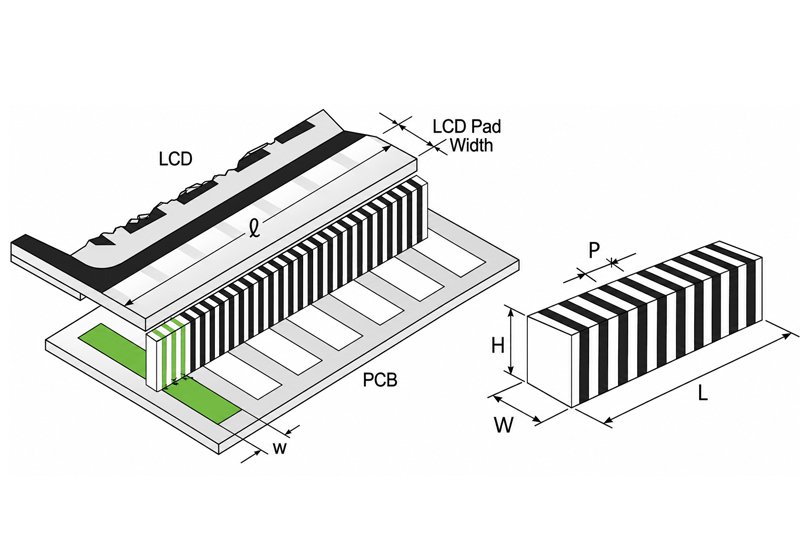
In display modules that use a silicone rubber zebra connector, contact reliability has a direct effect on product yield and long-term stability. When pitch becomes smaller than 0.6 mm, the PCB gold fingers and LCD glass electrodes leave very little room for alignment error. If the conductor width and the insulation gap are not balanced, the final product may show missing display segments, random characters, unstable contact, or shorted pins.
The most important layout rule is simple: for fine-pitch zebra strip connections, the conductor width and the adjacent insulation space should follow a Line/Space 1:1 relationship whenever possible.
What Is a Silicone Rubber Zebra Connector?
A silicone rubber zebra connector, also called a zebra strip or conductive rubber strip, is an elastomeric connector made from an insulating silicone body with parallel conductive paths inside it. The conductive paths are usually made with carbon-filled silicone or silver-filled silicone. The insulating silicone separates adjacent conductive channels and prevents lateral short circuits.
During assembly, the housing applies vertical compression to the connector. The conductive paths touch the PCB gold fingers on one side and the LCD ITO (indium tin oxide) electrodes on the other side. This creates an electrical path between the PCB and the LCD without soldering.
The PCB pads and LCD electrodes must align with the zebra strip’s conductive layers. The housing must then hold the strip at the intended compression despite assembly tolerances. Review this complete stack before specifying a custom connector.
Why Fine Pitch Makes Alignment Critical
The core challenge in a zebra connector design is alignment accuracy. As pitch becomes smaller, the safe tolerance window also becomes smaller. A small error in one part may look acceptable during incoming inspection, but the total assembly error can still become large enough to affect electrical contact.
The tolerance stack-up normally includes:
- PCB manufacturing tolerance.
- LCD glass electrode etching tolerance.
- Zebra connector conductive path pitch and verticality tolerance.
- Housing and frame assembly tolerance.
- Compression height and connector positioning tolerance.
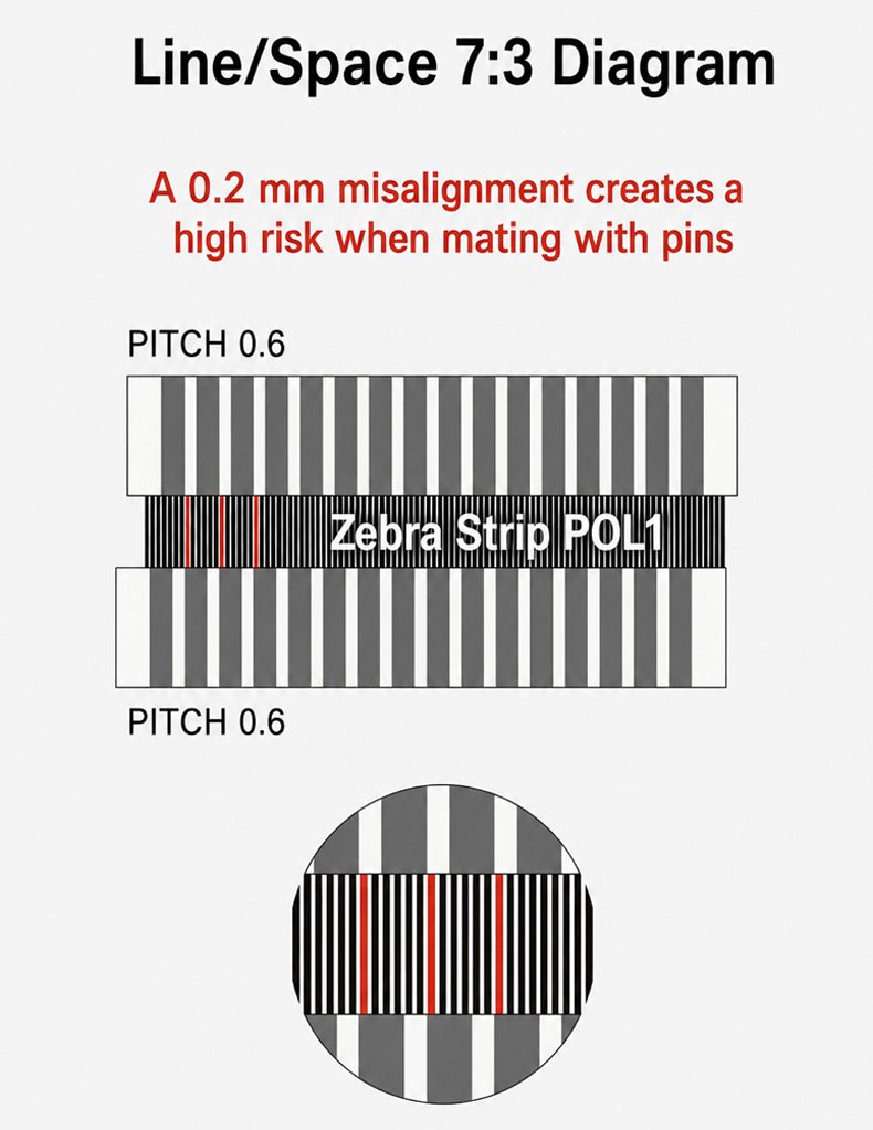
When pitch is below 0.6 mm, even a 0.05 mm error in several parts can become risky if the errors stack in the same direction. The result may be poor contact, missing display content, or signal shorting. This is why fine-pitch zebra strip design needs a system-level tolerance review.
The Line/Space 1:1 Design Rule
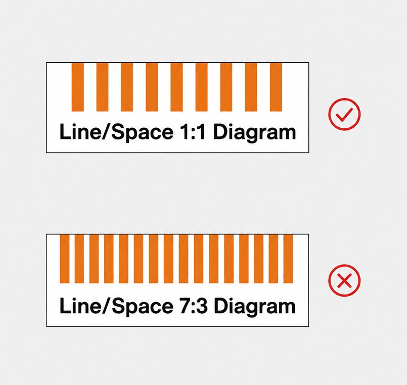
Line/Space 1:1 means the width of one conductive pad is equal to the insulation gap next to it. This rule should be applied to both sides of the connection: the PCB gold fingers and the LCD ITO electrodes.
- Line: the width of one conductive pad or electrode. In fine-pitch designs, keep it equal to the adjacent space.
- Space: the insulating gap between adjacent conductive pads. Keep it equal to the adjacent line.
- Pitch: one full conductor and insulation cycle. Review it together with the zebra strip conductive and insulating cycle.
If the PCB line width is larger than the space width, a wide gold finger may cover several conductive paths when alignment shifts. It can bridge another LCD electrode that should remain isolated. This creates a crossed-pin or short-circuit risk.
If the line is too narrow, the contact area becomes smaller. This can increase contact resistance and raise the risk of an open circuit. The 1:1 rule balances these two risks: it keeps enough contact area while still preserving insulation clearance.
Why 1:1 Layout Improves the Tolerance Window
When the PCB side and LCD side both use a strict Line/Space 1:1 design, their electrode pattern matches the conductive and insulating cycle of the zebra connector more predictably. This gives the assembly a wider process window.
The benefit is tolerance margin. If the line and space have equal width, the alignment shift must reach or exceed the width of one space before a short becomes likely. That gives the assembly more room to absorb small errors from the PCB, LCD, connector, and housing.
This is especially important for small LCD modules, meters, handheld devices, compact control panels, and other products where rework is difficult after assembly.
What Can Go Wrong Without 1:1 Design
Fine-pitch zebra connector assemblies usually fail for practical reasons, not because the connector material cannot conduct. Common causes include narrow pads, excessive pad width, poor symmetry between PCB and LCD electrodes, low compression, housing shift, or unreviewed cumulative tolerance.
Missing display segments often mean the contact area is too small or the alignment offset is too large. Check the line width, compression height, and zebra strip position before changing the connector material.
Random characters usually point to intermittent contact between the PCB, connector, and LCD. In this case, review compression height and cumulative tolerance across the full assembly.
Shorted pins can happen when one pad bridges multiple conductive paths after offset. The Line/Space 1:1 rule and a worst-case alignment check help reduce this risk.
High contact resistance is often caused by a narrow pad, low pressure, contamination, or poor surface contact. Review contact area, pressure, and cleanliness together.
Design Rules for Pitch 0.6 mm and Below
For fine-pitch LCD-to-PCB connections, the following rules help reduce contact risk before tooling and production begin.
| Design Area | Recommendation | Why It Matters |
|---|---|---|
| Line/Space rule | Use Line/Space 1:1 on the PCB and LCD electrode layout | This gives the connection the largest practical alignment tolerance window |
| Two-side symmetry | Keep PCB and LCD electrode designs matched | The connector contacts both sides with the same conductive and insulating cycle |
| Tolerance stack-up | Calculate the worst-case offset from PCB, LCD, connector, and housing tolerances | Confirms that the maximum shift stays inside the safe margin |
| Supplier specification | Send the same design rule to the PCB maker, LCD glass supplier, and connector supplier | Prevents each supplier from optimizing only its own part |
The first rule should be controlled at the layout and Gerber stage. If the Line/Space ratio is corrected only after sampling, the project may need a PCB revision, LCD glass revision, or new connector review.
Communicating the Specification to Suppliers
Many zebra connector issues start before production. The connector supplier may optimize the strip, while the PCB and LCD suppliers follow separate drawing rules. If these requirements are not aligned early, each part may pass inspection but the final assembly may still fail.
At the component selection and tooling stage, define the key requirements in writing:
- Zebra connector pitch and pitch tolerance.
- Conductive and insulating path structure.
- Connector height and recommended compression ratio.
- PCB pad line and space width.
- LCD electrode line and space width.
- Housing positioning features.
- Inspection method for contact and display function.
This does not need to be complicated. A simple drawing note can often prevent costly sampling issues: “PCB and LCD electrodes must follow Line/Space 1:1 for the zebra connector contact area, and total worst-case offset must stay within the approved tolerance window.”
Conclusion
Reliable contact requires the housing to keep the PCB and LCD aligned while compressing the connector correctly. At pitches of 0.6 mm or below, the Line/Space 1:1 rule provides more allowance for alignment error while maintaining contact area.
The best practice is simple: define the pad geometry early, keep both sides symmetrical, calculate cumulative tolerance, and share the same specification with the PCB, LCD, and connector suppliers before sampling begins.
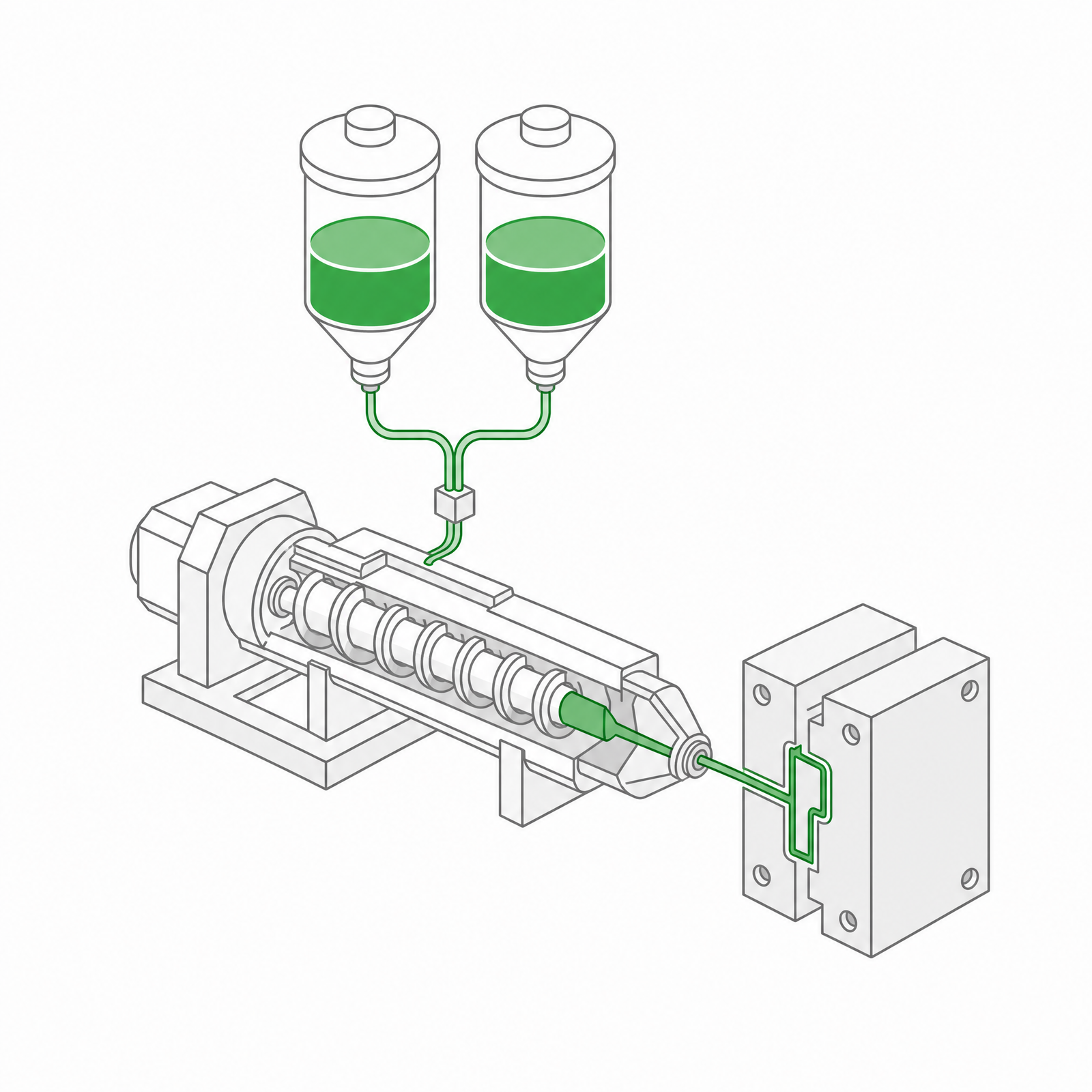 LSR Injection Molding
 Silicone Rubber Overmolding
 Compression Molding
 Silicone Rubber Extrusion
 In-house Tooling